Spacer glass
Outline
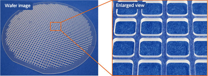
Suitable for multilayer packaging by combining with semiconductor wafers such as MEMS devices.

Features

Improve bonding yield with device wafers
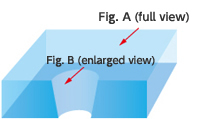
Control sagging around the holes
Minimize chipping size
- ≦10μm is available
Options
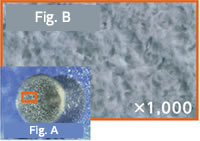
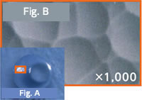
Remove microcracks from machined surface to control the particles
- Prevent malfunctions in bonding with MEMS devices
※Please scroll to the side.
| Standard specifications | |
|---|---|
| Material | Glass |
| Glass size | ≦φ200mm |
| Min. thickness | 0.15mm |
| Thickness tolerance | ±0.01mm |
| Min. hole size | φ0.3mm |
| Window shape | upon request |
| Window size tolerance | ±0.02mm |
| Chipping size | ≦100μm |
| Cross-section shape | Straight / Taper / Step |
| Metallization process | Available |
Note: These are standard specifications.
In case you have any request other than these, please feel free to contact us.


End user market / Applications
Projector
- Display devices for projectors,etc
Semiconductor
- RF-MEMS switches.
- Image sensors,etc
AV/Mobile
- RF-switches/relays for mobile devices such as smartphones, portable video games, digital cameras, car navigation systems,
Automotive
- Pressure sensors, Acceleration sensors.
- Gyroscopes,etc
- LED,etc
Biotechnology/Medical
- Analytical chips for DNA/drug-discovery-screening analyzers,etc
- Microreactors for biochemical reaction/electrophoresis analyzers,etc
- Bioreactors for chemical sensors, microorganism-detection sensors,etc
- Industrial gas-detection sensors,etc
