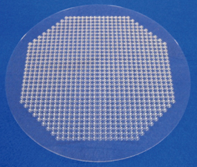
Micro-hole glass
Outline
Anodic bonding with a silicon wafer can result in solving the out-gas issue. It can be used in the wafer-level-packaging (WLP) process.
Features
Micro-hole processing
- min. size φ0.1mm
Max. glass size φ300 mm
(Some processes are only available up to ø200 mm wafer max.)
Improve bonding yield of device wafers
Suppress sagging around the holes
Minimize chipping size
- ≦10μm is available
※Please scroll to the side.
| Standard specifications | |
|---|---|
| Material | Glass |
| Glass size | ≦φ300mm(*) |
| Min. thickness | 0.15mm |
| Thickness tolerance | ±0.01mm |
| Min. hole size | φ0.1mm |
| Hole shape | upon request |
| Hole size tolerance | ±0.02mm |
| Chipping | ≦100μm |
| Cross section shape | Straight / Taper / Step |
| Metallization process | Available |
Note: These are standard specifications.
In case you have any request except for this, please feel free to contact us.
Sagging comparison
Sharp edge type
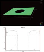
| Sagging size | |
| Width | <10μm |
| Depth | <0.1μm |
Standard type
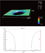
| Sagging size | |
| Width | >400μm |
| Depth | >0.7μm |
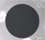
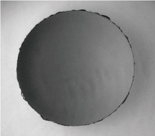
Chipping comparison
Less-chipping type
Standard type
End user market / Applications
Automotive
- Pressure sensors, Acceleration sensors.
- Gyroscopes,etc
Semiconductors
- RF-MEMS switches.
- Image sensors,etc