Silicon products
Outline
Both “Cross-edge” technology and quality assurance system make it possible to realize the highly-reliable silicon products. We continue to supply silicon parts which can meet the technological innovation our customers are handling.

Feature
Major advantages
By adopting ultrapure silicon materials (monocrystal/polycrystal), our products can minimize the risk of contamination and maintain your high-quality processes.
As our products have the same characteristics (thermal conductivity, specific heat, coefficient of thermal expansion) as silicon wafer, damage to your product is suppressed much lower than any other material, leading to the improvement in the yield and productivity of your process.
Excellent thermal conductivity realizes the uniform distribution of film and its stability.
Outstanding heat-resistance and corrosion-resistance make it possible to enhance the durability in high temperature process.
High precision processing with complicated shapes can meet various customers' needs.
Ultrapure silicon products can enhance reliability of product without delamination of the coating which may cause contamination.
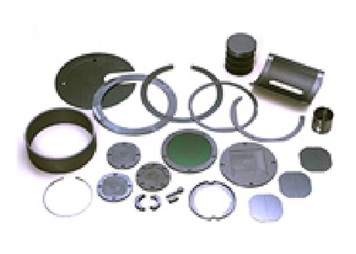
Silicon products
| CVD susceptors, Rings for various equipment |
Focus rings | Cleaning jigs |
| Wall plates in the implantation dome | Tubes | Pins |
| Optical waveguide wafer jigs for various devices | Tables | Nozzles |
Silicon wafer for dicing test
We sell silicon wafers for pre-dicing, experiment and evaluation purposes.
【Standard specifications】
Surface: Mirror finished surface on the one side.
Following size and thickness are available.
| Diameter | Thickness(μm) | ||
|---|---|---|---|
| 4in | ①400〜700 | ②500±25 | ③530±25 |
| 5in | ①500〜700 | ②550±25 | ③625±25 |
| 6in | ①500〜700 | ②450±50 | ③625±25 |
| 8in | ①725〜25 | ②725±50 | |
| 12in | ①775±50 | ||
Regular package style: Coin stack. (Case delivery is also available)
【Others】
For front-end use, particle-controlled silicon wafer is also available. (particle spec.: less than 30 pieces of particles more than 0.2 μm)
Samples of processing silicon/ceramics products
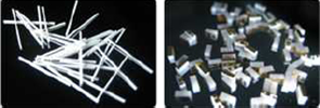
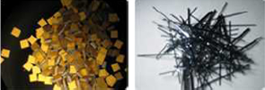
We apply our high-precision technology to a variety of materials such as silicon, Al2O3, AlN, sapphire, etc. Some of the examples are dicing into bars of 100 &mu m-wide with chipping suppressed, and burr-less metalized ceramic dicing.


